Okay, you’ve got your marvelous antenna shining in the morning sun. Beautiful and brand new ground station, maybe even connected to the SatNOGs network, stands proudly in your backyard (or hangs from the balcony of a multi-family block of flats). Everything seems fine, except… it’s not perfect when it comes to satellites’ reception. The signal is barely visible and you can only dream about its demodulation. Why? Is there anything you can do to improve it? The answer is: probably yes. LNA and filter to the rescue!
❯ Disclaimer: I’m not a professional radioelectronics person. In fact – I’m a newbie! Interested in radio waves, building antennas, and listening to the satellites’ signal, but still, absolutely not an expert in this matter. I consulted this blog post with my friends who are working in electronics on a daily basis however, I didn’t want to make it all too advanced – I just wrote down everything in a way I understood it. So please, don’t treat this article as an arbitrary truth. It was written with the intention that it can serve as an introduction to the topic and as a starting point for beginners who would like to build their own LNA with a filter for their ground station.
I just hope it may be helpful for you – if you are at the beginning of your radio-electronics-ground-station journey. Enjoy!
If you just want to get the tutorial, go to the second section – and if you want to discover why putting an LNA with a filter in your ground station may be a good idea and read about my motivation for designing it, head to the first chapter. Or, do you just wish to see the real project? Visit a Github repository with a board design. Enjoy!
Section 1: theory and other stuff
🎶 Somebody once told me, the world radio stuff is gonna roll me 🎶
Radio electronics is hard. Even if you try to calculate all parameters precisely during designing the board, it may turn out that after soldering and measuring it will not be perfect anyway. Everything matters – PCB’s height, route’s length and width, even distances between components (!). Why am I highlighting this? So that you don’t get discouraged if something doesn’t work out the first time. I needed two iterations to get a satisfactory result, and this was still in cooperation with great electronics – I can easily imagine that without them, there could be even over a dozen ;).
Why do we need an LNA and filter anyway?
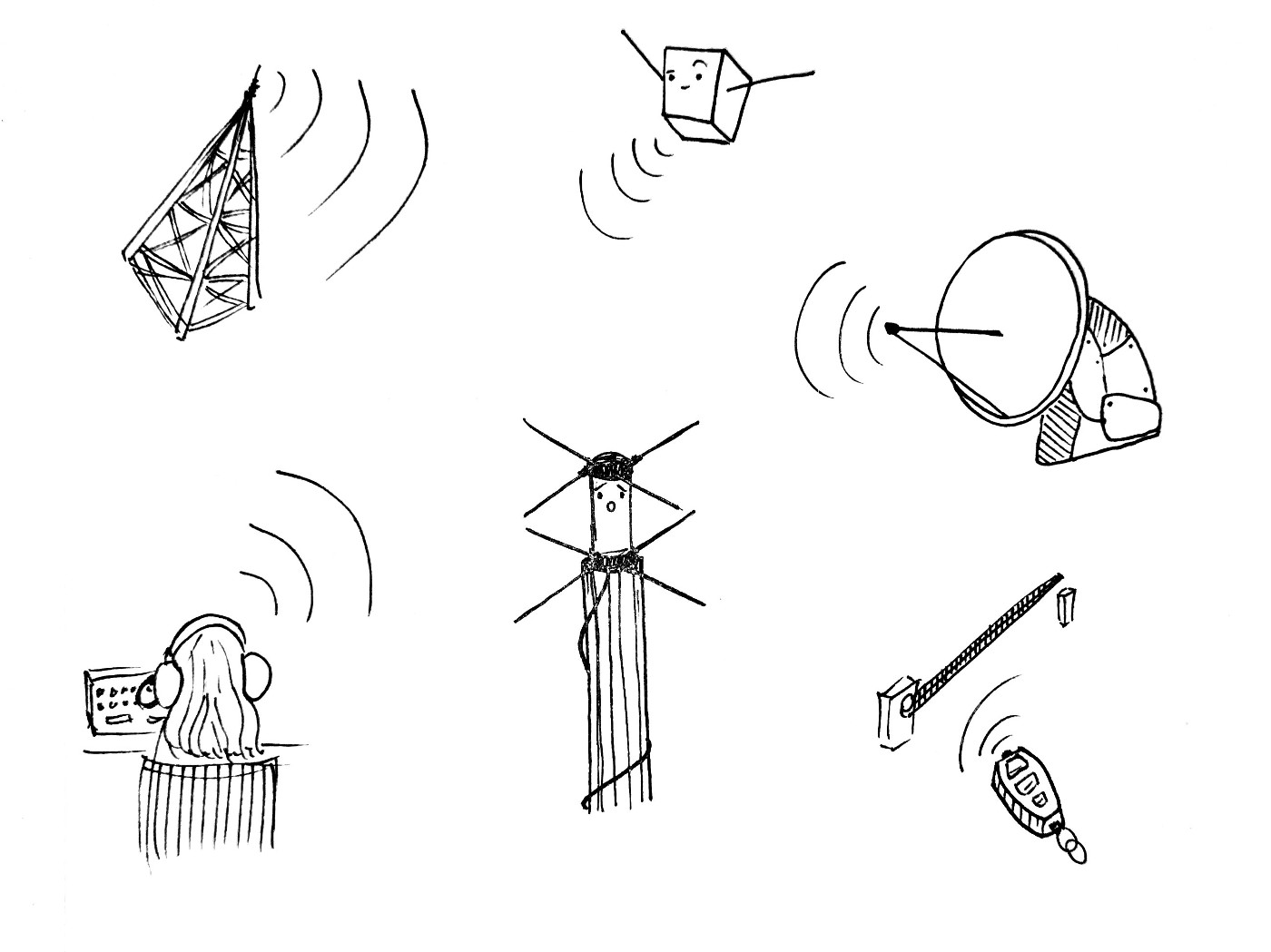
Fig. 1 - Too much signal!
As this is written explicitly on the RTL-SDR website, it is a wide frequency software-defined radio with a frequency range around 500 kHz – 1766 MHz (with small differences between dongle’s variants). It basically means that it will try to receive every signal in this range. Of course, reception outcome will vary depending on the antenna capabilities and its SWR. A properly tuned antenna will partially reflect not-matching frequencies, but every signal that goes through and is outside the wanted range can “clog up” the SDR, causing problems with the reception quality. And that’s where the LNA and bandpass filter come to the rescue – they will limit the received signal to the specific range and amplify only this range. Radio music, gates’ remote controllers, HAM radio enthusiasts having fun on the nearby frequencies… it all gets cut off. And you can listen only to the things you want. Sounds good, doesn’t it? (like, you know, literally ;)).
The setup
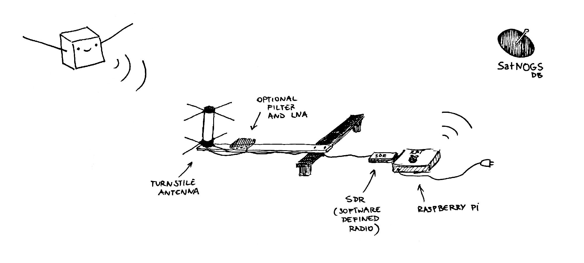
Fig. 2 - Ground station setup with LNA+filter
In the setup from Fig. 2, you can see the antenna and LNA+filter placed as close to each other as possible. Amplifying the signal as soon as it enters the source is very important for good reception. Every cable introduces some signal loss and the longer it is, the bigger the loss (you can compute it by yourself for your specific cable using its datasheet). As the amplifier doesn’t distinguish between a meaningful signal and noise, it amplifies both, so noise temperature is also a significant factor in the reception quality. I won’t go into detail but you can read more about it e.g. here or here.
Did I place the LNA close to the antenna? In fact, nope. The device requires powering it with 5V and to achieve this, I would have to install an additional power line on the balcony. I hadn’t got a chance to do it until now, so it stayed connected directly to the SDR-RTL, being powered from a USB connector on Raspberry Pi. According to the theory though, the results could be better if I did it, so I encourage you to try both configurations and see which one is better (and I’m gonna try it one day too!).
DIY? I can buy it on eBay!
Yes, you can. And I also bought it :). There are a few LNAs available for 400-440 MHz, mostly Chinese or custom ones – with prices starting with 10$ and going up as high as someone is willing to pay. I ordered an inexpensive one to compare its performance to my design – after waiting for around three months (😬), a board arrived and was placed in the ground station setup. The reception turned out to be slightly better than without any – I was able to demodulate and decode a little more signals than before.
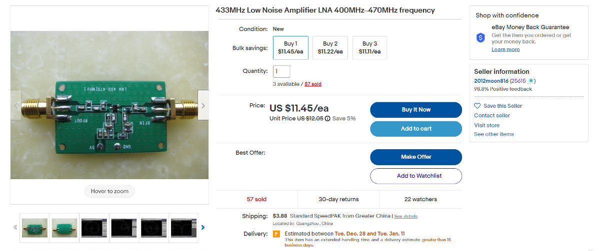
Fig. 3 - Buy LNA from eBay they said, it will be fun they said
In November this year I had a chance to measure both off-the-shelf LNA and my own creation with professional equipment. It turned out that the purchased device was… poorer quality than mine. It was okay, it was working and amplified the signal but didn’t filter it properly. In short: not great, not terrible.
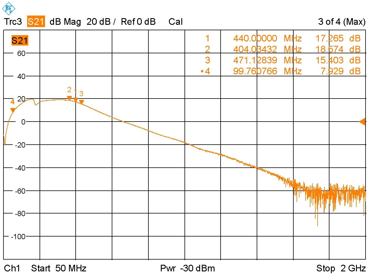
Fig. 4 - Cheap eBay LNA+filter S21 measurement. Not great, not terrible.
I’m sure that there are some good quality LNA+filters available to buy somewhere but their prices start with 50$ and up. I didn’t want to spend that much money for a ready-made device – I apparently preferred to spend… more money on my own PCBs, components and get frustrated over a mediocre first version 😬. Apparently, everyone gets what they deserve :).
Anyway, LNA+filter is an interesting radio electronics project that can be quite easy to understand (on the basic level) and not very complicated to test experimentally (if you own a ground station – it’s only a matter of attaching one more device to the setup). Most components used for making are widely accessible resistors, capacitors, and coils with one IC (amplifier) in the middle.
The only issue can be with performing the proper evaluation, as the majority of the measurement devices are extremely expensive. There are cheaper ones (e.g. NanoVNA) that should be quite good for our needs (but they have some limitations, unfortunately). But if you have a possibility to measure your solution with any tool, it’s worth doing it – it gives some information on what could be improved in future revisions. Experimental testing is fun too but there are many factors that affect the quality of reception and with little data, it can be difficult to determine whether it was the LNA with the filter that really helped.
Can this design be adapted for other frequencies? For example, 146 MHz?
Yes! The only thing that has to be done is a recalculation of the filter components’ values to match the VHF frequency range. In theory, you should be able to retune it for any frequency you need, excluding very high frequencies (>2 GHz), as the higher they get, the radio stuff gets more and more complicated. But 146 MHz should work nicely (and I also plan to make it one day).
Section 2: LNA + bandpass filter tutorial
How to design a 400-440 Mhz LNA with a filter?
Here you can find a detailed description of the process of making a 70 cm band low noise amplifier with a filter. When designing yours, you can follow my path or look directly at the finished project and base your solution on it – any option is good.
What are you probably going to need?
- LC filter design tool – I used a simple online one
- electronics design software – KiCad in my case; I love it and it’s open-source!
- Git – it’s better not to lose your hard work, right?
- Saturn PCB – or other PCB calculator to compute board’s parameters
- PCB manufacturer
- components for the board
- measuring equipment – to verify if your LNA is working as it should
- …patience 😬
The below steps should be repeated until your design is satisfactory. Good luck!
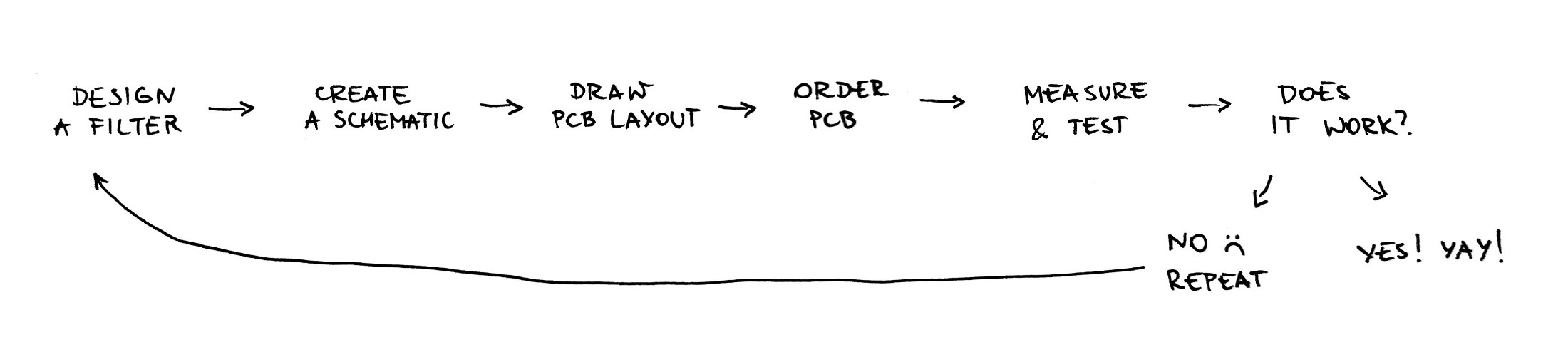
Fig. 5 - Process of making of LNA with filter. Repeat until satisfied :)
1. Design a bandpass filter
I started this adventure by designing a filter for the LNA. As it was explained in the previous section – without it, the amplifier would enhance all frequencies, so the solution wouldn’t help much with getting rid of unwanted signals.
LC filter uses coils and capacitors to cut or pass specific frequency bands. I found an easy online tool to perform a calculation of what components should be used to build one – on rf-tools website. I chose a bandpass Chebyshev one, with 2nd order. Theoretically, a bigger order would give us a more precise one, but it would require more parts and I wanted to keep the project as simple as I could. As you can see in the Fig. X, it’s important to select proper frequencies, impedance, and standard component values – to avoid situations in which the calculator tells us to buy something that doesn’t exist.
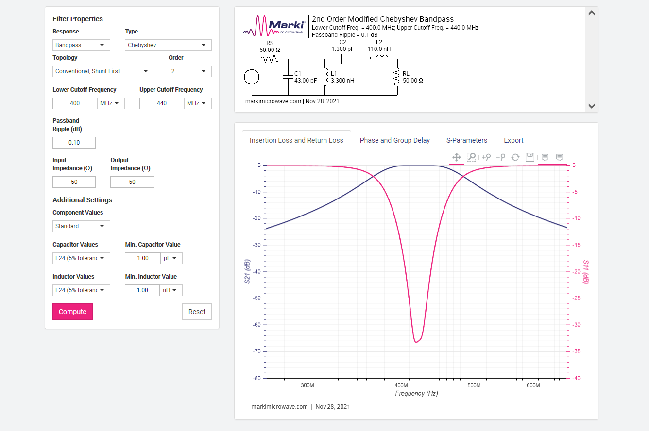
Fig. 6 - First filter design. Feeling like a pro.
After clicking COMPUTE, you are given schematics and a characteristics chart with S11 (return loss) and S21 (gain) values for the specific frequencies. I won’t go into detail about what they are – if you want to know more, you can always watch e.g. this video. The intuitive thing is – we want S11 to be as small as possible and S21 as high as possible in the chosen frequency scope. It will then mean that the filter is going to pass signals from this range and block signals that are outside of it – and this is, in simple words, our goal.
After performing a calculation, have a look into the components’ properties too. Try to avoid very low capacitors’ and coils’ values as the routes possess some non-zero capacity and inductance themselves and the filter will become hard to tune later.
2. Create a schematic
Time to create a new KiCad project. Of course, use any design software you like – I’m using KiCad as it’s open-source, intuitive and, what’s most important, it saves files in the text form, and they can be easily tracked with git. Here I can highlight that I strongly recommend using git as a version control system for every project you do, not only for programming :). More info and some tutorials can be found on its website – for hosting you can explore Github, Gitlab, or whatever you wish.
Okay, back to electronics.
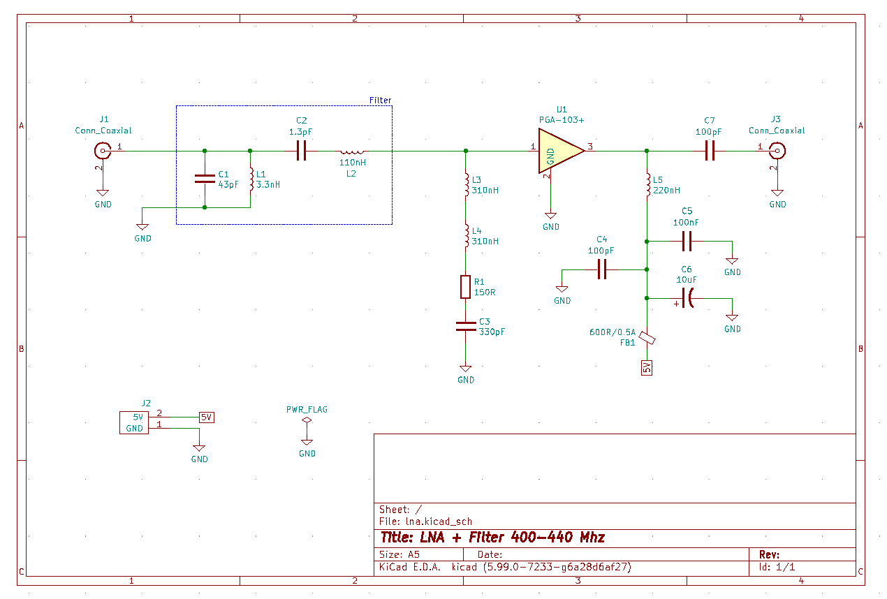
Fig. 7 - First version schematics. Don't copy this!
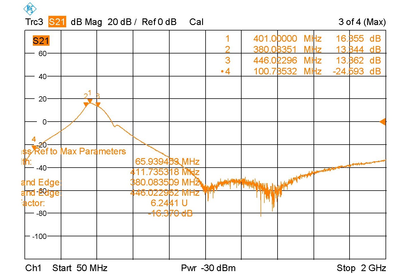
Fig. 8 - First version measurement - it's tuned too low. Could be better and will be better.
In Fig. 7, you can see the very first version of the LNA project. I redrew the filter exactly as it was calculated and marked it with a blue rectangle. On the right side, there is an LNA part of the schematics – I chose PGA-103+ as the amplifier and drew the rest as it was stated in its datasheet (adding only one more capacitor and a ferrite bead on the power line to filter random noises). As PGA-103+ needs a 5V power supply, I included a pin header (J2) to be able to provide both the power and GND.
The first version turned out to be tuned for lower frequencies than expected (Fig. 8). The peak was around 400 MHz and amplification was weaker than anticipated, so I decided to create a second revision. The iteration was performed after measuring the first revision with NanoVNA and consultation with a specialist. The overall schematics stayed the same but some components’ values in the filter part were changed (as you can see in Fig. 9). They were selected experimentally, this time without much confidence in the calculations of the filter design tool (they served only as a base). The most significant changes were made to the PCB itself, but more on that in a moment.
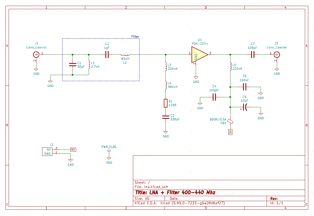
Fig. 9 - Second version schematics with adjusted components' values.
3. Draw a PCB layout
For me, this step is the best fun. Drawing a PCB layout is de-stressing and has something akin to art – maybe that’s why I like it so much.
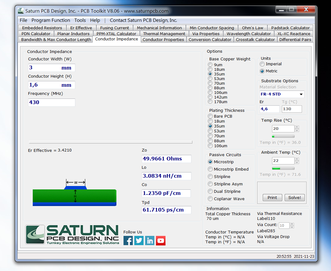
Fig. 10 - Saturn PCB calculation for 1st version.
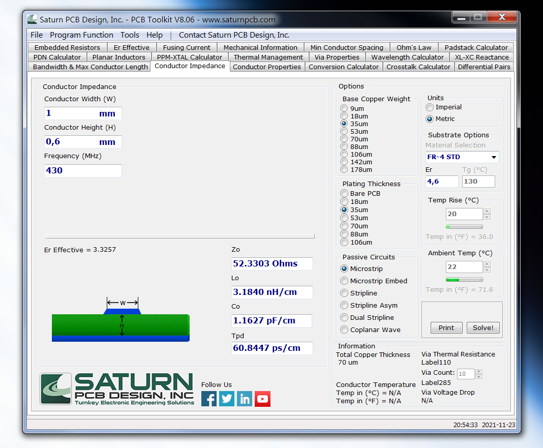
Fig. 11 - Saturn PCB calculation for 2nd version.
First, you can use a PCB calculator (Saturn PCB or other) to calculate route width to match the 50 Ohms impedance. For the first version of the board, I used a standard PCB height (1.6 mm), which caused the conductor width to be as big as 3 mm. In the second iteration, I decided to choose 0.6 mm PCB height, which made the route 3 times narrower (1 mm). It looked better and worked better, so I highly recommend it. Why, you may ask? Well, 3 millimeters is quite a large value. Components’ pads are usually about 1 mm in width, so the path of the signal turned out to be sometimes narrow and sometimes wide – it may have had an impact on the performance. In the second revision, I put all the filter parts desperately close to each other and it would be very hard to draw a 3 mm wide line between them. It was then more reasonable to use a narrower route and it required changing the PCB height too. Remember that every millimeter of the route has a non-zero capacity and inductance, so it’s important to avoid big distances between parts. Note it, it’s important!
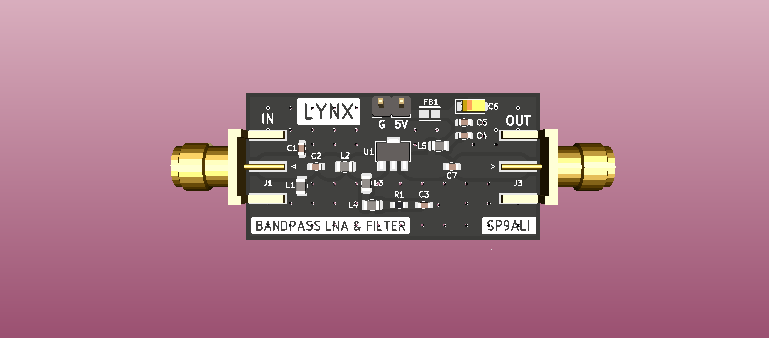
Fig. 12 - Lynx, the first version.
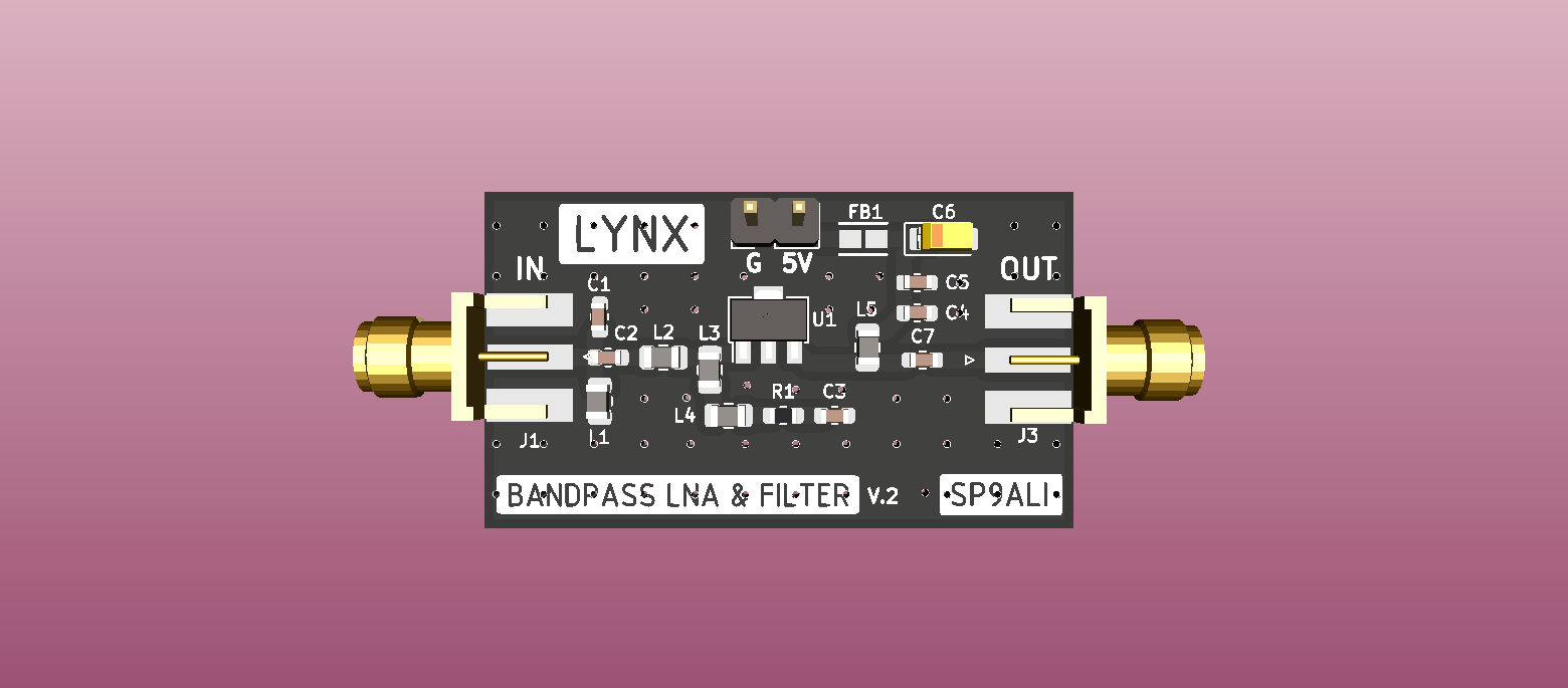
Fig. 13 - Lynx, the second version, components close to each other and 1 mm route.
As you can see in Fig. 13, the board has many holes in it. It is a common practice in the radio electronics world to use them to help control unwanted electromagnetic interference that appears between the sides of the board by reducing GND impedance. It’s not the most important thing with the lower frequencies (and 430 MHz is not very high), so it’s not required – but it’s a good practice, so I added them.
Apart from holes, I think there is nothing unusual in the board – two SMA connectors (IN and OUT), an amplifier in the middle, and goldpins to be able to supply power. There is no information about the frequency written on the PCB on purpose, as you can adapt it to any range by adjusting components’ values to your needs.
4. Order your PCB and components
Time to order your PCB! There are several companies in Europe, China or USA that provide a manufacturer service for electronic boards. Choose any factory you like, remember only about selecting proper settings:
- PCB height: 0.6 mm
- copper weight: 1 oz (~35um)
- material type: FR-4 standard
- your favourite board colour :)
I usually use JLC PCB and PCBWay, but there should be no differences between them or other manufacturers (at least for amateur needs). From my experience with Chinese factories: it’s good to order at least 10 boards even if you need one or two because sometimes pads happen to be damaged on a few of them.
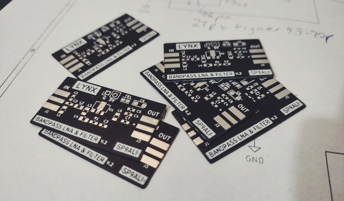
Fig. 14 - Second version boards, just lying around. Thin as potato chips.
When it comes to parts – at the moment of writing (December 2021), we are suffering from the crisis in electronic components all over the world. Because of the pandemic, speculative buying, and probably other less obvious reasons, many parts are not available to buy or became extremely expensive in the last months. Luckily, the LNA+filter project consists almost only of very popular and basic components – coils, capacitors, and resistors – that should still be obtainable and cheap :). You have to specifically find only two SMA connectors and one PGA-103+. Full BOM can be generated from the KiCad project on my Github.
Small advice: it’s good to order more components’ values that are needed for the project. If there is a need for a 47 pF capacitor, I recommend buying also 33 pF, 39 pF, and 56 pF capacitors – during the tuning, you may be forced to try a few configurations to find a perfect one. Trimmer capacitors are a great solution too, as you can change their values easily without re-soldering the component.
5. Measure & test
After waiting for the PCB to arrive (with Chinese manufacturers’ shipping to Europe it can take even a few weeks), the time will come for the most important step – measurements and tests. As I mentioned earlier, the professional equipment for this step is absurdly expensive but there are some cheaper alternatives available that can be good enough for amateur needs.
I measured the first revision with NanoVNA (Fig. 15) and defined the first problem – as I wrote earlier, it was tuned to lower frequencies than expected (around 380-400 MHz). It turned out that even by changing the values of the capacitors and coils, I am not able to adjust the filter to 435 MHz. Without NanoVNA, I wouldn’t know that something doesn’t work as it should – placing the LNA in the setup resulted in quite good observations, comparable to the eBay one.
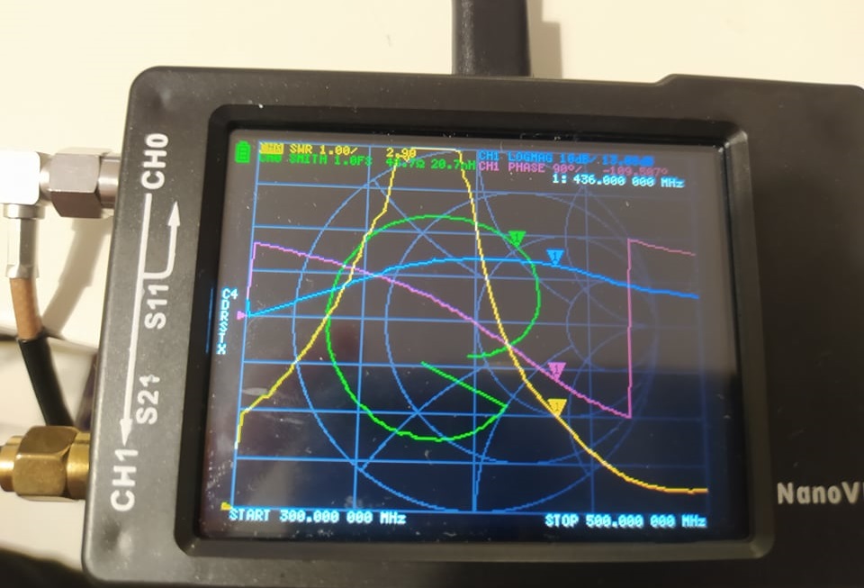
Fig. 15 - Measurement of the 1st version with NanoVNA. Have in mind that the scale differs in both pictures (this and Fig. 16).
Fig. 16 - Measurement of the 1st version with professional equipment. Yes, this image was already here, good spot!
A decision was made to create the second revision of the board – thinner and with components very close to each other (to avoid parasitic capacitance and inductance). To tune it, again NanoVNA was initially utilised, but I wanted to measure it in a more advanced way. Thanks to the courtesy of Grzesiek, who let me use his equipment, I managed to test it ✨professionally✨. According to the measurements, the second version is noticeably better than the first – and definitely higher-level than the bought one. Yay!
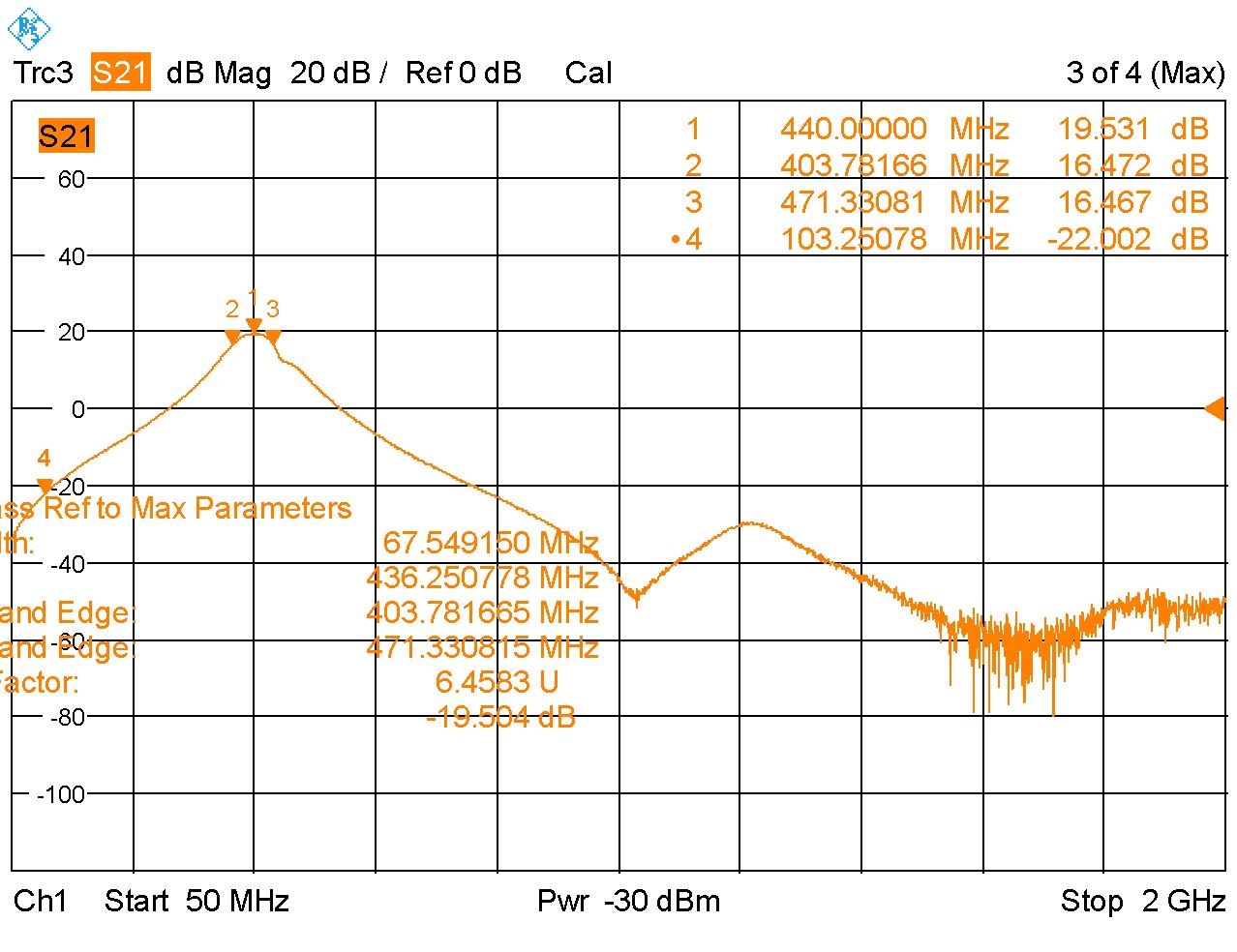
Fig. 17 - Measurement of the 2nd version with professional equipment (S21).
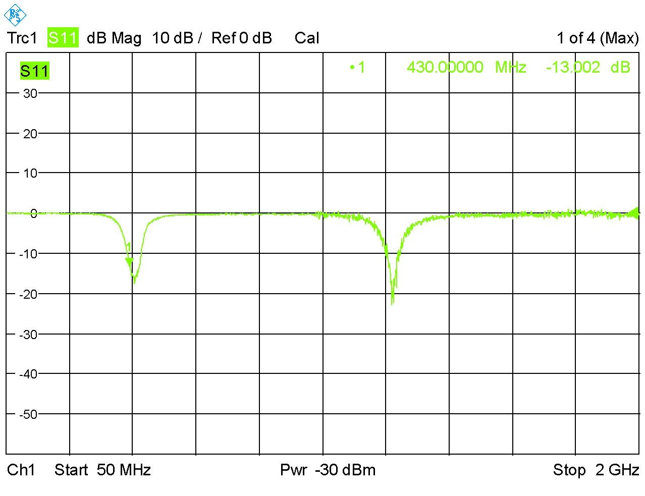
Fig. 18 - Measurement of the 2nd version with professional equipment (S11).
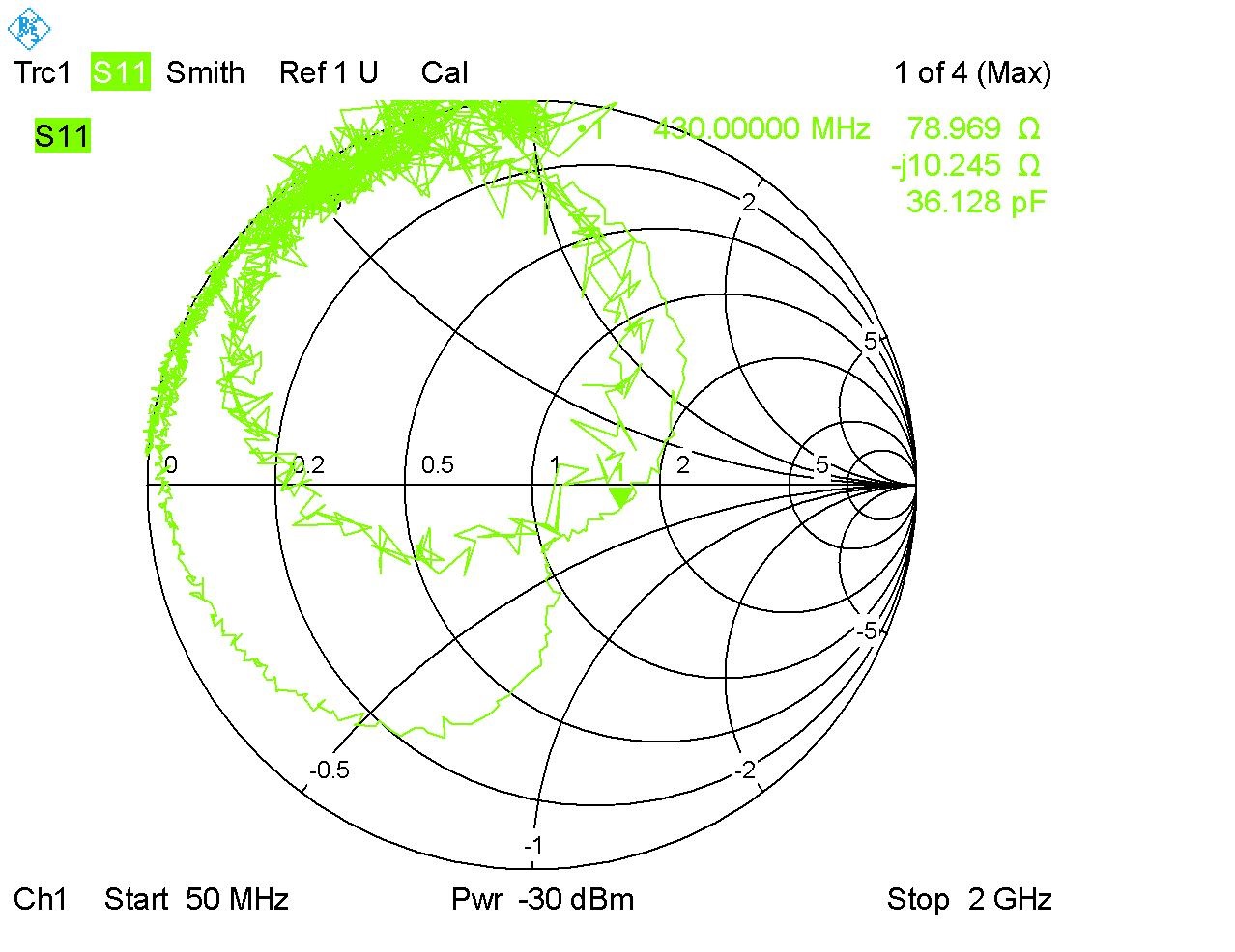
Fig. 19 - Measurement of the 2nd version with professional equipment (S11, Smith chart).
As you can see in the figures above – the second version has a visibly higher gain than the first one (by a few dBs) and the filter itself is nicely tuned exactly to the frequencies I wanted (400-440 MHz). Of course, it is still not perfect and I wouldn’t call it state-of-the-art but it’s quite a result a newbie can be proud of :).
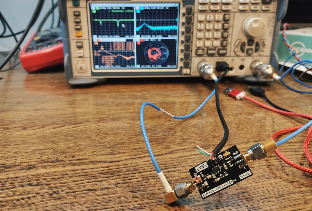
Fig. 20 - Measuring = fun. As long as everything works, of course.
Summarizing...
I’m using the Lynx board daily – it’s permanently connected to my SatNOGS station. And overall, I’m quite satisfied with the outcome. Taking into consideration that my antenna is placed on the balcony near the big city centre and it only “sees” one side of the sky, the observations are pretty good anyway. And there is a visible difference with and without the LNA, so it was definitely a project worth doing.
Glad that you made it to this point! If you have any questions about the design or thoughts on how it can be improved, don’t hesitate to leave a comment. I also strongly encourage you to build your own solutions and share the results – it’s great to have the possibility to read about other people's experiences and see their amazing work.
If you are looking for some inspiration about the antenna, have a look at my previous tutorial or at the Libre Space Community forum (there are many interesting designs out there). And if you ever plan to build your own LNA with a bandpass filter based on mine – totally do, I’m looking forward to admiring your creations! :) It’s fun and you can learn a lot, so the best combination there is.
See the whole project on Github:

Thanks!
Thank you very much for the a(n)ttention! I hope that this guide can be used for beginners who are planning to design their own LNA with a bandpass filter. Have fun and 73 :)
Finally, tremendous thanks go to Piotr and Grzesiek – without your help, the process of trying and learning would definitely take more than a few months. High-five!
Sources and recommended links
- https://www.rfcafe.com/references/electrical/noise-figure.htm, [access: 7.12.2021]
- https://www.rtl-sdr.com/about-rtl-sdr/, [access: 7.12.2021]
- https://rf-tools.com/lc-filter/, [access: 7.12.2021]
- https://www.youtube.com/watch?v=-Pi0UbErHTY, [access: 7.12.2021]
- https://www.youtube.com/watch?v=BijMGKbT0Wk, [access: 7.12.2021]
- https://www.youtube.com/watch?v=rUDMo7hwihs, [access: 7.12.2021]
- https://www.youtube.com/watch?v=ENy_zg9dX5c, [access: 7.12.2021]
- https://docs.kicad.org/5.1/en/getting_started_in_kicad/getting_started_in_kicad.html, [access: 7.12.2021]
- https://www.proto-electronics.com/blog/pcb-design-hints-rf-pcb, [access: 7.12.2021]
- https://network.satnogs.org/, [access: 7.12.2021]